Shreetu´s and Gebi´s Manuscript on Perovksite X-Ray Detectors published by Nature Photonics
Lead halide perovskite semiconductors have an inherently high X-ray absorption cross-section, dedicating them for advanced X-Ray detection.
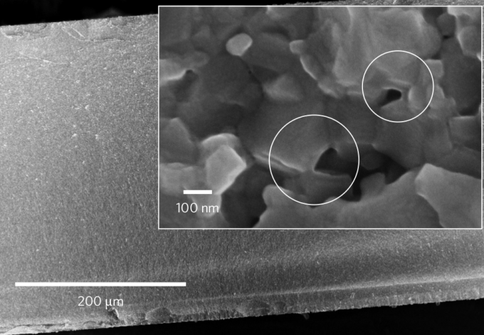
However, the processing of several-hundred-micrometres-thick high-quality crystalline perovskite films over a large area has been
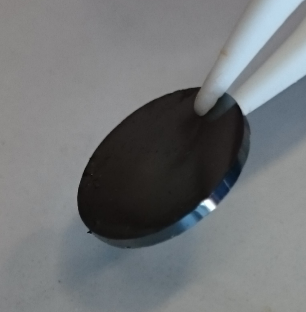
unresolved so far. To overcome this problem, Shreetu and Gebi developed in cooperation with Siemens a mechanical sintering process to fabricate
polycrystalline MAPbI3 wafers with millimeter thickness and well-defined crystallinity. These wafer pellets performed amazingly
well in comparison to state of the art CdTe based X-Ray detectors and set a new benchmark for perovskite based X-Ray conversion.