NGSE5, Day 2: Tutorial Session
The fourth tutorial session at the NGSE4 was kicked off by Henri Snaith from the University of Oxford with a great introductory lecture. Prof. Snaith lectured on the basics and the development of Perovskite materials for PV-applications leading up to the design of Si/PSK-Tandem Solar cells, ending with insights into the mechanisms for degradation and stability for perovskites. In the end Prof. Snaith shared some new results of imaging Perovskite with TEM with surprising detail.
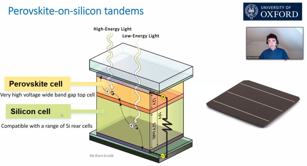
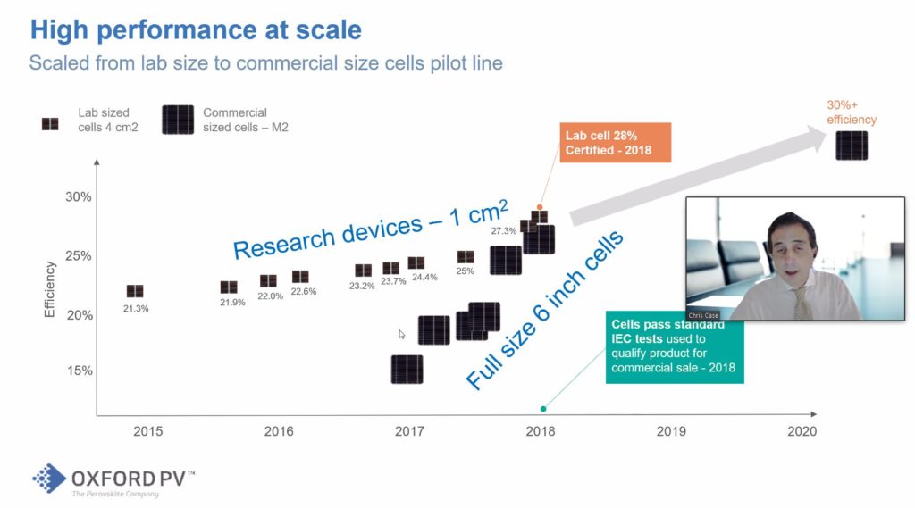
Dr. Chris Case, CTO of Oxford PV, followed the lecture by Prof. Snaith with a great overview on the challenges of upscaling a new technology like Si/PSK Tandems to a commercial scale, as well as the string of achievements Oxford PV has made towards this goal. By focusing on adding an additional layer of perovskite on a standard Si-Wafer they have been able to scale up very fast by using much existing technology.
A further talk on upscaling perovskite production was provided by Bin Fan from GCL Nano. Bin Fan begins his talk by pointing out the amazing progress in PSk-Stability that has been achieved. He also points out, that a pure PSK-module will actually contain less lead than a Si-module. An advantage of scaling PSK is that it is more like scaling a display production, rather than scaling a Si-production. Currently GCL Nano is preparing a 100 MWp line working on 1mx2m modules. Bin Fan presents calculations showing that a GW-facility for PSK will be more than 3x cheaper than an equivalent facility for Si-modules and 8x cheaper than a CIGS facility. Bin Fan also believes that there are interesting opportunities for voltage matched Si/PSK tandems, as well as pure PSK tandems from a cost perspective.
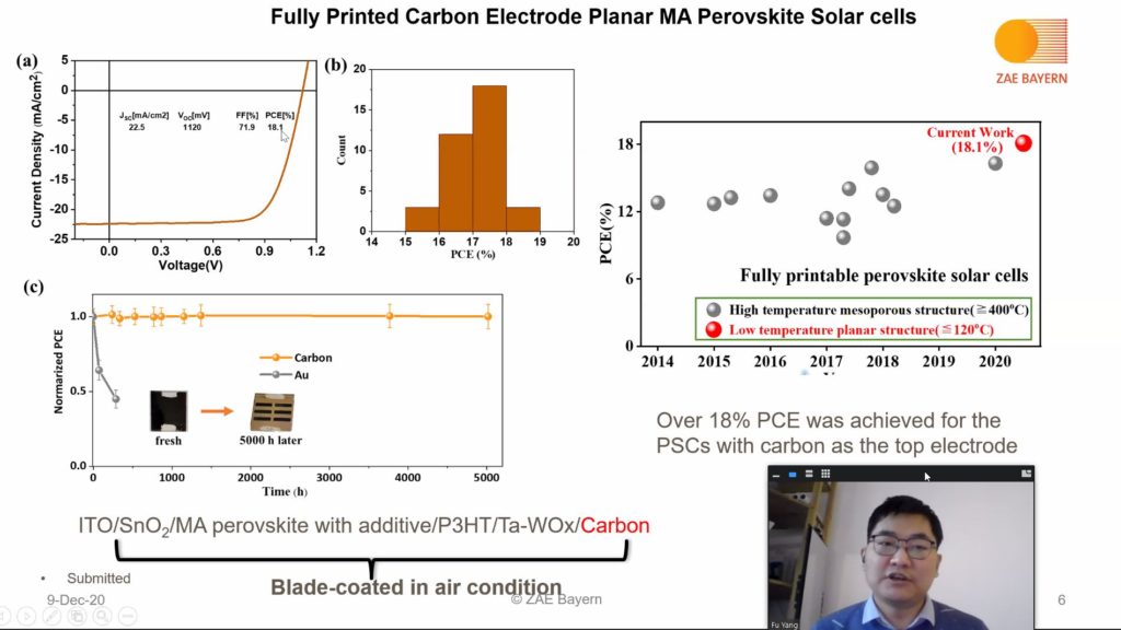
Dr. Fu Yang from ZAE Bayern presented the upscaling developments for fully printed perovskites for production on Roll-to-Roll equipment. With printed Electrods made from Carbon so far more than 18% efficiency could be achieved in cells with good efficiency. The technology was also scaled to modules with 16.9% efficiency.
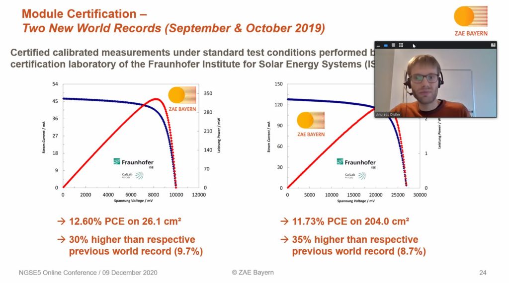
Dr. Andreas Distler followed by describing the results of the production group for OPV modules at ZAE Bayern. In his presentation he starts in by pointing out how losses accumulate when going from lab-to-fab for a flexible module. The largest share of the losses comes from a change of substrate. Beyond that Dr. Distler detailed the process for making a record OPV-Module with 12.6%.
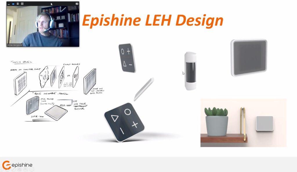
In the next Tutorial of the session Jonas Bergquist from Epishine is outlining their approach to the market for applications of OPV. Epishine is focussing on indoor IOT products, mainly for wireless connected sensors. Epishine has developed a custom production process for OPV based on lamination in order to make the parallel resistance as large as possible to achieve best possible indoor performance.
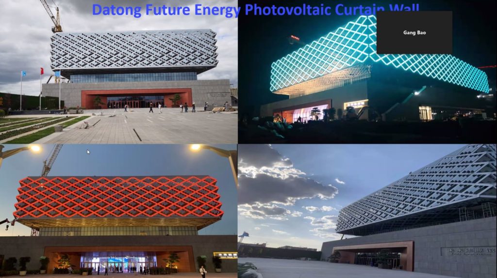
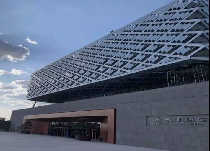
The final presentation in the tutorial sessions is given by Gang Bao the CTO of Advanced Solar Tech is giving an introduction to the use of CdTe in BIPV applications. Advanced Solar Tech is a manufacturer of CdTe Modules and is capable of manufacturing both opaque and semitransparent. Gang Bao presents an impressive portfolio of buildings which utilize their modules to achieve stunning architecture while still producing energy from seamlessly integrated, semitransparent of colored modules.