SOPSEM group overtakes Ultra-High Vacuum Semiconductor Technology with simple Inkjet Printing
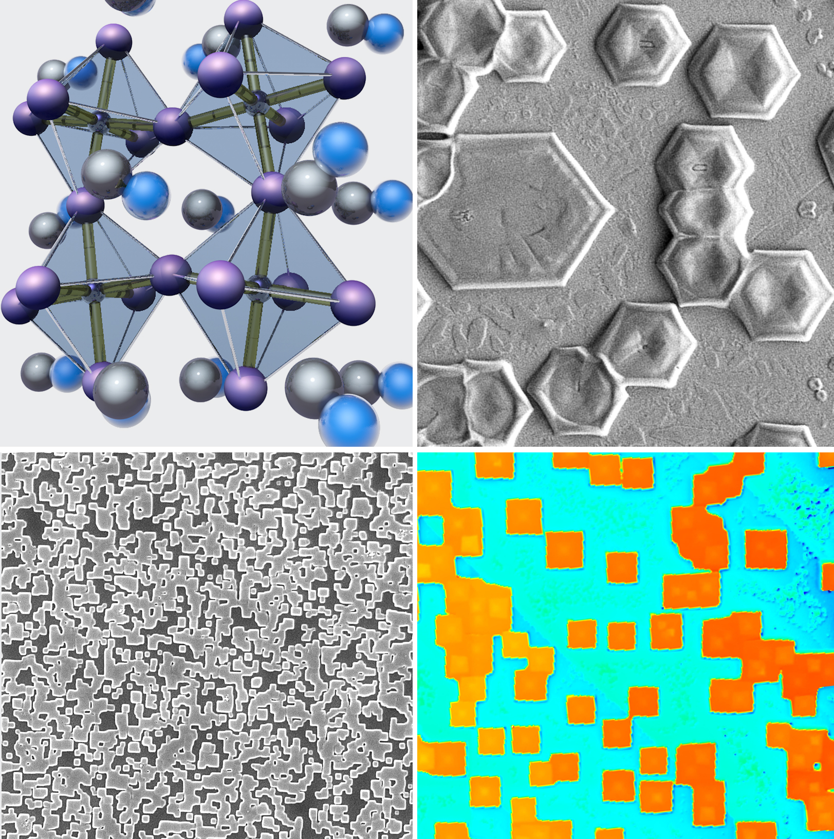
Prof. Heiss’ group SOPSEM (SOlution-Processed SEMiconductors), in collaboration within the IMEET department and several other FAU WW-s groups, has demonstrated a new approach of metal halide perovskites (MHP) heteroepitaxial crystal growth based on cheap and scalable inkjet printing. The paper is published in Advanced Functional Materials Journal. The developed inkjet printing technology has the potential to impact the whole semiconductor industry. The intrinsic physical properties of MHP, like solubilizing in polar solvents and tolerance to internal defects, make them perfect for processing with printing techniques. The Inkjet printing by itself represents a drop‐on‐demand digital, additive, and very flexible printing technique utilized for the cost‐effective fabrication of different electronic devices. Applying epitaxial deposition principles for inkjet printing may unveil irreproachable device performance, which is only achieved by 1000 times more expensive ultra-high vacuum deposition technologies. SOPSEM studied in detail the boundary conditions like precursor compositions, temperature, environment parameters, and the crystal structures relation of grown material to the substrate for achieving optional selective epitaxial growth starting from separated single crystallites and ending with a full closed single-crystalline compact film. Even though the scope of the study was the development of epitaxial inkjet printing technology of MHP, the SOPSEM group found also that the MHP hetero‐epitaxial structures exhibit bright luminescence and extended cubic crystal phase stability due to interfacial lattice anchoring by the substrates. The epitaxial inkjet printing method has the potential to be applied to a large variety of semiconductors for extremely cheap, large-scale, single‐crystal electronic device developments and fabrication