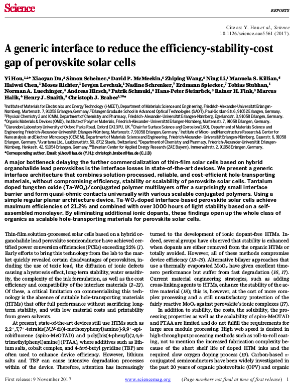
Yi’s article on his 21.2% perovskite material system is published in the journal of science
The mineral perovskite is considered a miracle semiconductor in optoelectronics and especially in solar technology. Highly efficient, but so far hardly suitable for everyday use due to incompatible interfaces. I-MEET researcher Dr. Yi Hou is working on resolving the problem by creating a material system that allows the production of efficient and durable perovskite-based solar cells. With the help of special nanoparticles, he developed a generic process with which the boundary layers in the solar cell can be very precisely doped.
Since all processes take place at low temperature and from solution, this invention has the potential to revolutionize printed solar technology. Yi published the research results in the journal of Science. (doi: 10.1126 / science.aao5561, Full Text)
Perovskite is considered a particularly suitable semiconductor to convert sunlight into electricity. For example, the material is particularly easy to process. While standard semiconductors such as silicon are either melt-removed or deposited in high-vacuum systems, perovskite can be applied from the solution at normal room temperature, for example by means of printing and coating processes.
With a thin layer of tantalum-tungsten oxide (Ta-WOx) nanoparticles, Yi has now succeeded in further increasing the efficiency of the material – to a value of even 21.2 percent. This degree of efficiency has not yet been achieved by research for this component architecture. Ta-WOx/conjugated polymer multilayers offer a small interface barrier and universally form ohmic contacts with various scalable conjugated polymers. This work will stimulate broad interest, which is beneficial not only to perovskite photovoltaics but also to the conventional as well as the emerging photovoltaic technologies.
External Links:
- Full Text
- https://www.fau.eu/2017/11/21/wissenschaft/breakthrough-in-solar-technology/
- https://www.fau.de/2017/11/news/wissenschaft/durchbruch-in-der-solartechnologie/ (German)
- https://erlangenheute.wordpress.com/2017/11/20/durchbruch-in-der-solartechnologie-fau-experteninterview/ (German)
- http://science.sciencemag.org/content/early/2017/11/08/science.aao5561
- https://www.openpr.de/news/979275/FAU-Forscher-entwickeln-neues-Materialsystem-fuer-effiziente-und-langlebige-Solarzellen.html (German)
- http://www.advancedsciencenews.com/perovskite-perspectives-yi-hou-christoph-brabec-talk-hysteresis/

