Gebi demonstrates a “state of the art” perovksite X-Ray detector fabricated via a simple melt process
The current state-of-the-art X-ray to current converter technology is based on Cd(Zn)Te. The into crystalline wafer processed material, offers ideal properties but requires demanding production processes such as zone melting, the Bridgman method or epitaxial growth. Beside the high costs, most limiting is the small size of the Cd(Zn)Te wafers. On the other hand, metal-halide perovskites for direct X-ray to current converter showed a rapid progress and are approaching the performance of single crystalline Cd(Zn)Te detectors.
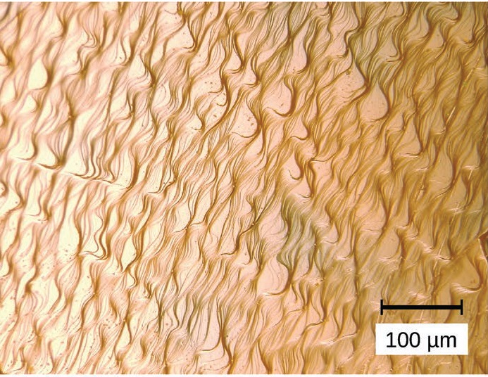
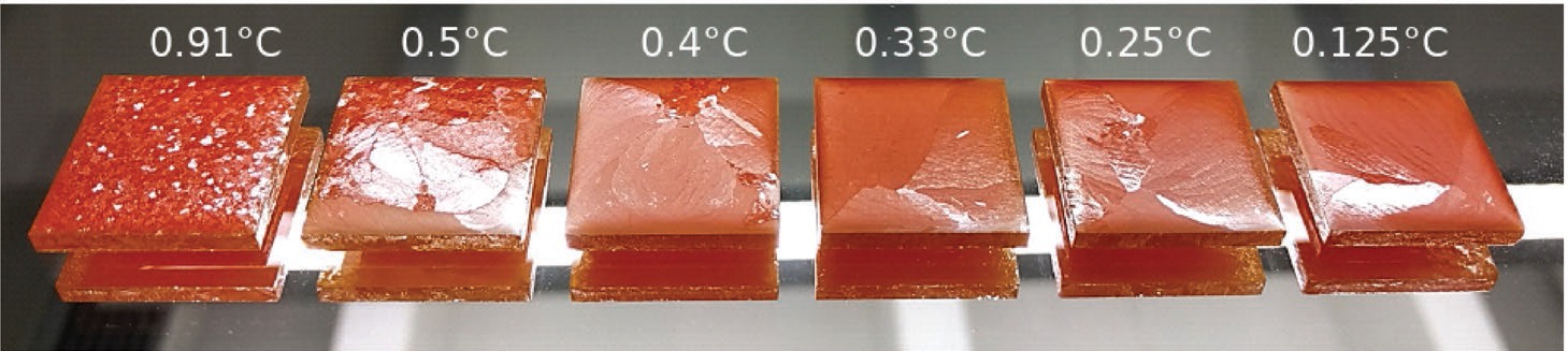
In his recent paper in Advanced Materials Interfaces, Gebi demonstrate excellent electro-optical properties of single crystalline CsPbBr3 layers processed by a simple melting process of CsPbBr3 powder directly on substrates of any size. Although the principles of this method go back on an ancient technique, the “vitreous enamel” glazings, only few reports regarded this concept for perovskite processing.
Gebi built X-Ray detectors from the molten films and found state of the art performance, comparable to high end CZT detectors. The findings are published in the current issue of Advanced Materials Interfaces.