• Skip navigation
  • Skip to navigation
  • Skip to the bottom
Simulate organization breadcrumb open Simulate organization breadcrumb close
i-MEET
  • FAUTo the central FAU website
  • Department WW
  • HI-ERN
  • Emerging PV Reports Initiative
  • POPULAR
  • FAU Solar

i-MEET

Navigation Navigation close
  • Home
  • Institute
    • History
    • Mission
    • Research Groups
      • Optoelectronic Devices, Photovoltaics & Energy
    • Projects
      • iPEN: Innovative Photonics Education in Nanotechnology
    • Equipment
    • Teaching
      • Lectures
      • Colloquium
      • Colloquium: History
    Portal Institute
  • Publications
  • People
    • Prof. Dr. Christoph J. Brabec
      • Publications
      • Lectures
    • Prof. Dr. Wolfgang Heiss
    • Prof. Dr. Olga Kasian
    • Prof. Dr.-Ing. Peter Wellmann
    • Prof. i.R. Dr. rer.nat. Albrecht Winnacker
    • Priv.-Doz. Dr. Miroslaw Batentschuk
    • Priv.-Doz. Dr. Hans-Joachim Egelhaaf
    Portal People
  • Jobs&Theses
    • i-MEET open positions
    • Theses
    • HiWis
    • External
    Portal Jobs
  • Contact
    • Privacy Statement
    • Legal Notice
    • Accessibility
    Portal Contact
  1. Home
  2. Institute
  3. Research Groups
  4. Crystal Growth

Crystal Growth

In page navigation: Institute
  • History
    • Archival photos of the department
  • Mission
  • Projects
    • iPEN: Innovative Photonics Education in Nanotechnology
    • SFB953
  • Research Groups
    • Optoelectronic Devices, Photovoltaics & Energy
    • Light & Phosphors
    • Solution Processed Semiconductors
    • Crystal Growth
  • Equipment
  • Teaching
    • Lectures
    • Seminar on Solar Energy
    • Colloquium
    • Colloquium: History

Crystal Growth

Crystal Growth Lab

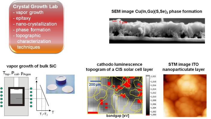
The research activities in the crystal growth & characterization lab of Prof. Dr.-Ing. Peter Wellmann at the electronic materials and energy technology division of the materials department (University of Erlangen-Nuremberg) are devoted to crystal growth, epitaxy and characterization of modern topics in semiconductor technology. Materials for energy saving are in the current focus of research:

  1. Silicon carbide for power electronic devices is a promising candidate for energy saving during electric power conversion.
  2. The CI(G)S thin film solar cell materials recently have reached a maturity that allows the realization of commercial solar panels.
  3. Printed electronic layers offer a great potential of a wide range of (opto-)electronic and photovoltaic device applications.

In the field of characterization a large variety of electrical, spectroscopic and structural techniques are used which serve the better understanding of materials processing. Special emphasis is put on topographic methods. In all fields service for industrial and institutional partners may be provided.


crystal_growth_lab

Friedrich-Alexander-Universität
Erlangen-Nürnberg

Schlossplatz 4
91054 Erlangen
  • Jobs
  • Contact
  • Privacy Statement
  • Legal Notice
  • Accessibility
  • RSS Feed
  • YouTube
Up